Why silicon is neither a metal nor an insulator: the band gap Eg, doping and the p–n junction behind diodes, solar cells, transistors and LEDs, whose colour follows λ=hc/Eg.
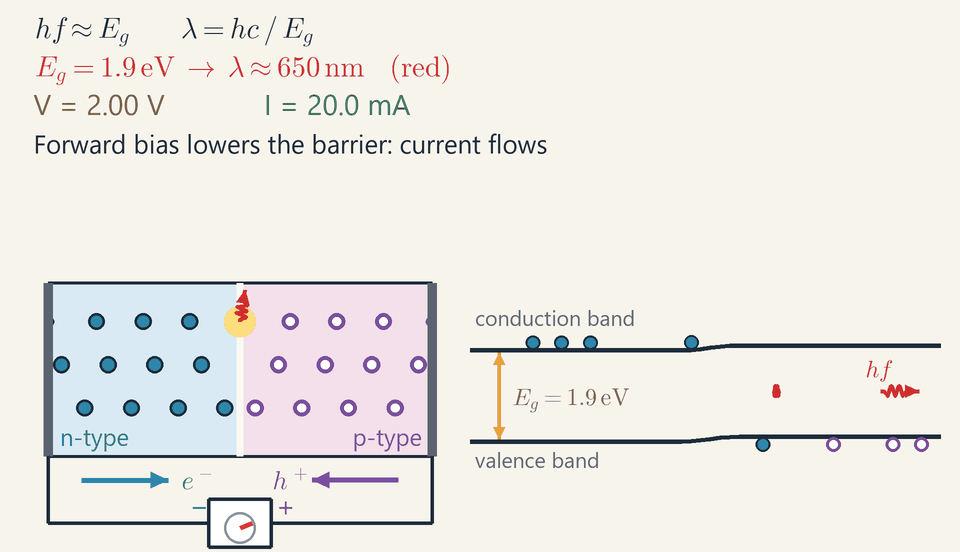
A red LED chip: as the voltage rises, electrons and holes flow to the p–n junction, recombine and send out photons whose energy is close to the band gap.
Conductors such as copper let charge flow, insulators such as glass do not; semiconductors such as silicon sit in between.
A hole is a gap where an electron is missing; as neighbours jump into it, the gap moves like a positive charge.
Doping adds a pinch of another element: n-type material gets spare electrons, p-type material gets holes.
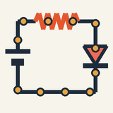
A p–n junction is a one-way valve for current (a diode): it conducts only when the battery faces the right way.
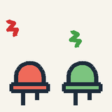
In an LED each electron that drops into a hole gives out a flash of light; the material, not the battery, sets the colour.
A copper wire carries charge easily because some of its electrons belong to no particular atom: it is a conductor. In glass every electron stays with its atom: an insulator. Silicon, the material of computer chips, sits in between: a semiconductor.
Step 1. In pure silicon almost every electron is held in a bond between neighbouring atoms. A little heat or light shakes a few loose, and each leaves a gap called a hole. When a neighbour jumps into the gap, the gap moves the other way, so a hole travels like a positive charge.
Step 2. Engineers mix in a pinch of another element; this is called doping. One kind of impurity brings spare electrons (n-type, n for negative); another kind leaves holes (p-type, p for positive).
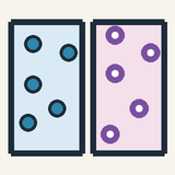
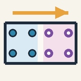
Step 3. Put the two types side by side and you have a p–n junction. In the animation the blue dots on the left are spare electrons and the rings on the right are holes. A thin empty layer between them acts like a wall. While the voltage is low, nothing crosses; at about 2 volts both kinds of charge stream towards the middle.
Step 4. An electron that drops into a hole loses energy, and that energy leaves as a tiny flash of light, just as an atom gives out a photon when one of its electrons falls to a lower level. This is a light-emitting diode (LED). The size of the drop, and so the colour, is set by the material.
Check yourself: connect the battery the wrong way round. Does the LED light up? No: the wall gets thicker and almost no current flows. A junction is a one-way valve for current, called a diode. Shine light on it instead and it drives a current: a solar cell.
Intermediate
Key ideas
The conduction band lies a gap Eg above the filled valence band (Si: Eg=1.12eV; GaAs: 1.42eV).
The depletion layer forms a barrier: forward bias (p to +) lowers it and current flows; reverse bias raises it.
Recombination emits a photon with hf≈Eg, so λ=hc/Eg≈1240eV⋅nm/Eg (1.9eV→650nm).
LED current rises very steeply with voltage, so an LED always needs a series resistor.
Bands, gaps and holes
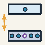
A copper wire carries an electric current easily and glass hardly at all, while silicon, the material of computer chips, sits in between. An electron bound to a single atom can have only certain energies. In a crystal every atomic level spreads into a band of closely spaced levels. The bonding electrons fill the valence band; above it lies the conduction band, where electrons move freely, and between the two the band gap Eg, energies that no electron in a perfect crystal can have.
A full band carries no current, since each electron moving one way is matched by one moving the other way. A metal conducts because its highest occupied band is only partly filled. An insulator has a full valence band and a wide gap, 5.5 eV in diamond; a semiconductor has a narrow one: 1.12 eV in silicon, 1.42 eV in gallium arsenide (GaAs), 1.9 eV in the red LED of the animation.
At room temperature the thermal energy kBT≈0.026eV lifts only about 1010 electrons per cubic centimetre across the gap of silicon, out of 5×10²² atoms. Each leaves an empty place in a bond, a hole; a neighbouring electron slips into it and the hole moves the other way, like a positive charge +e. The number of pairs doubles about every 10 K, so a pure semiconductor conducts better when hot, unlike a metal.
Doping: n-type and p-type
Doping controls the carriers. Phosphorus has five outer electrons, one more than the four bonds of silicon need; the spare one, held by only 0.045 eV, is freed by thermal motion at once. Phosphorus is a donor and makes n-type silicon, with electrons as majority carriers. Boron, with three, takes an electron from a neighbouring bond and leaves a hole: p-type silicon.
One phosphorus atom per five million silicon atoms gives 1016 free electrons per cubic centimetre, a million times the pure value. The holes become rarer, because so many electrons fill them, and the product of the two densities stays fixed: np=ni2,ni∝exp(−2kBTEg) Here ni≈1010cm−3 is the density in pure silicon, so the holes drop to p=1020/1016=104cm−3: they are the minority carriers.
The p–n junction and its band diagram
Join n-type and p-type regions in one crystal. Electrons diffuse into the p side and holes into the n side, where they recombine, leaving near the boundary only fixed ions: positive donors on the n side, negative acceptors on the p side. This depletion layer, a fraction of a micrometre thick, has no free carriers, and the field of its ions pushes carriers back until diffusion stops at a built-in voltage Vbi: about 0.7 V in silicon, 1.8 V in the animation's LED.
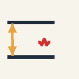
The band diagram in the animation draws this as a step, with electron energy upward: the upper line is the conduction band edge, the lower one the valence band edge, 1.9 eV apart (gold arrow). Both edges are higher on the p side, so an electron (blue dot) from the n side must climb the step, while a hole (ring), which floats up like a bubble, would have to sink down it. Unbiased, the step is 1.8 eV high and almost nothing crosses.
Bias, current and light
Forward bias (p side to +) works against the built-in voltage: the step shrinks, the depletion layer narrows and the current grows exponentially. Reverse bias raises the step, and only a tiny saturation current Is leaks through. The junction is a diode, a one-way valve. Four formulas do most of the work:
hf≈Eg
λ=Eghc≈Eg1240eV⋅nm
I=Is[exp(ηkBTeV)−1]
R=IVs−VF
A conduction electron that falls into a hole drops by about Eg and emits one photon; since hc≈1240eV⋅nm, dividing by the gap in electronvolts gives the wavelength in nanometres. In the diode equation the thermal voltage VT=kBT/e is 25.9 mV at 300 K, and the ideality factor η lies between 1 and 2: each extra 2.3ηVT (60 mV for η=1, 120 mV for η=2) multiplies the current by ten.
Worked example: the LED in the animation
The chip in the animation has Eg=1.9eV. Each photon carries about that energy, 1.9⋅1.602×10−19=3.04×10⁻¹⁹J, and its wavelength is λ≈1.9eV1240eV⋅nm≈653nm which the animation rounds to 650 nm: red light.
As the supply voltage V rises, the readout I stays below half a milliampere up to about 1.5 V, while the caption says the barrier is still high; it passes 1 mA at about 1.56 V and reaches 20 mA at 2.0 V. Half a volt multiplies the current more than fiftyfold. Meanwhile the band step shrinks from 1.8 eV to about 0.1 eV (the chip's resistance takes the other 0.3 V), the depletion layer narrows to a quarter of its width, and the e− and h+ arrows show carriers streaming in from both sides.
Each crossing electron gives at most one photon, so the current counts the photons: at 20 mA, I/e=0.020/(1.602×10−19)≈1.25×1017 per second, carrying at most 1.25×1017⋅3.04×10−19≈0.038W of light from 2.0⋅0.020=0.040W of electrical power. Whatever does not escape as light warms the chip.
Worked example: a resistor for a blue LED
A blue LED has a wider gap, Eg≈2.7eV (λ≈460nm), so it needs about 3.0 V rather than 2 V to carry 20 mA. You have a 5.0 V USB supply. A series resistor carries the same current and takes the rest of the voltage: R=IVs−VF=0.0205.0−3.0=100Ω It dissipates 2.0⋅0.020=0.040W, and the LED 3.0⋅0.020=0.060W.
Without it, the LED's own curve, far too steep, would set the current: in the animation half a volt changes the current fiftyfold, so 5 V across a bare LED would destroy it. With the resistor, an LED whose forward voltage is 3.1 V instead of 3.0 V still gets 1.9/100=0.019A: the resistor, not the LED, fixes the current.
Common mistakes
n-type silicon is not negatively charged: each phosphorus atom enters neutral, and when its fifth electron wanders off, a fixed positive ion stays behind.
A brighter LED does not give bluer light. The current sets the number of photons per second, about 1.25×10¹⁷ at 20 mA; the gap sets the energy of each.
A diode has no fixed resistance: the LED of the animation has V/I=1.5/0.00037≈4kΩ at 1.5 V but 2.0/0.020=100Ω at 2.0 V.
Reverse bias does not block at any voltage: beyond breakdown the reverse current shoots up, and LED data sheets allow only about 5 V in reverse.
Where you meet it
LED lamps, screens and traffic lights use the light of this lesson. A solar cell is the same junction doing the opposite job: light creates electron–hole pairs, and the field of the depletion layer drives them apart as a current, as in camera sensors and fibre-optic receivers. Transistors, built from junctions or a field-controlled channel, switch and amplify the signals in every chip. Compare Photoelectric Effect and Atomic Models: the Bohr Atom for the photon side, and DC Circuits and Ohm's Law for the circuit side.
Advanced
Key ideas
Hopping between atoms makes a band E=E0−2Acoska; near its edge electrons and holes move like free particles with an effective mass.
Pair creation ∝e−Eg/kBT balances annihilation ∝np: np=ni2, so doping raises one density and lowers the other.
Bias tips the balance of two flows: I=Is[exp(eV/ηkBT)−1]; the uphill flow grows exponentially, the downhill flow stays fixed.
The current grows tenfold per 2.3ηVT; since Is∝e−Eg/kBT, the knee sits just below Eg/e.
Light needs a direct gap (GaAs, InGaN), not Si; run backwards, the junction is a solar cell.
Bands from hopping between atoms
Everything a semiconductor does comes from one fact: its electrons are not tied to single atoms. To see how that produces bands of allowed energies separated by a gap, follow one electron in the simplest crystal there is, a straight chain of identical atoms.
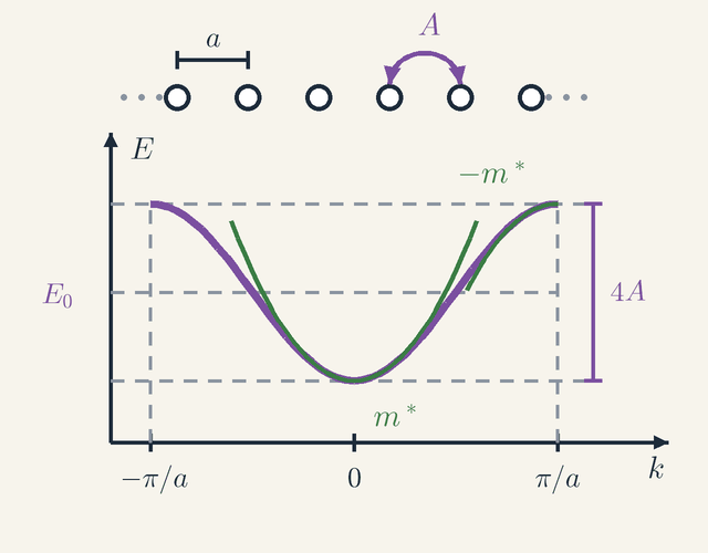
Figure 1. A chain of atoms a apart with hopping energy A (top) spreads the atomic level E0 into the band E=E0−2Acoska, of width 4A. The green parabolas match the band's curvature at its bottom (mass m∗) and at its top (−m∗).Legend
a
Spacing of the atoms in the chain.
m
A
Hopping energy: the coupling between two neighbouring atoms.
J
E
Energy of one wave state of the chain.
J
k
Wave number of that state: its amplitude on the atom at xn is proportional to eikxn.
m−1
E0
Energy level of an isolated atom; the band is centred on it.
J
4A
Width of the band, from E0−2A at k=0 to E0+2A at the edge.
J
π/a
Edge of the range of k needed: a k beyond it puts the same amplitudes on the atoms as one inside.
m−1
m∗
Effective mass at the bottom of the band, set by the curvature of the green parabola there; at the top the curvature is reversed, giving −m∗.
kg
The top of Figure 1 shows the chain. The atoms are a distance a apart, so atom number n sits at xn=na. On its own, each atom would hold the electron at the energy E0. Because the atoms are close, the electron can also hop to either neighbour; the curved double arrow marks this, and the hopping energy A measures how strongly two neighbouring atoms are coupled.
Since the electron can always leak to a neighbour, a state with the electron sitting on one atom cannot keep a fixed energy. A state of definite energy must give the electron an amplitude Cn on every atom. Its Schrödinger equation says: the energy times the amplitude on atom n equals E0 times that amplitude, minus A times the amplitudes on the two neighbours,
ECn=E0Cn−A(Cn+1+Cn−1)
Every atom has the same surroundings, so try a wave, Cn=eikxn, with wave number k. The two neighbours then carry eikxneika and eikxne−ika. The common factor eikxn cancels from both sides, and since eika+e−ika=2coska, what is left is
E=E0−2Acoska
This is the curve in the lower part of Figure 1: the energy E of each wave against its wave number k. Only k from −π/a to π/a is needed. Adding 2π/a to k multiplies the amplitude on atom n by ei2πn=1, so it gives back the same wave. At k=0 every atom has the same amplitude, and the energy is lowest, E0−2A: the bottom of the band. At k=±π/a the sign of the amplitude flips from one atom to the next, and the energy is highest, E0+2A. The single atomic level E0, the dashed line halfway up, has spread into a band of width 4A, the bracket on the right.
Each atomic level spreads into its own band in this way, and between two bands lie energies that no wave in the chain can have: a band gap. In a semiconductor at absolute zero the electrons exactly fill one band, the valence band, and leave the next one, the conduction band, empty. The distance from the top of the valence band to the bottom of the conduction band is the gap Eg, 1.12 eV in silicon.
Near the bottom of a band only small k matter, and there coska≈1−21(ka)2. Putting this into the band gives
E≈E0−2A+Aa2k2
Apart from the constant, this has the form of the kinetic energy of a free particle, ℏ2k2/2m, where ℏ is the reduced Planck constant. So an electron near the bottom of the band moves through the crystal like a free particle, but with an effective mass
m∗=2Aa2ℏ2
The stronger the hopping, the lighter the electron. A coupling of 1 eV between atoms 0.3 nm apart gives m∗≈0.42me, where me is the mass of a free electron; measured values run from 0.07me (electrons in GaAs) to about me. In Figure 1 the green parabola at the bottom, labelled m∗, is this approximation. It hugs the band near k=0 and parts from it farther out, where the cosine flattens.
At the top of the band the cosine curves the other way. The second green parabola, labelled −m∗, fits the band there: an electron near the top has a negative effective mass, so a force accelerates it backwards. Now take a band that is full except for one electron missing near its top. A full band carries no current, because every electron moving one way is matched by one moving the other way. The band with a gap in it therefore behaves like the missing electron with both its charge and its mass reversed: charge +e instead of −e, mass +m∗ instead of −m∗. This missing electron is a hole.
The hole is a genuine quasiparticle, a particle-like excitation of the crystal: the Hall voltage of p-type material has the sign expected for positive carriers. Lifting an electron from the top of the valence band to the bottom of the conduction band makes one free electron and one hole, so Eg is the least energy that creates an electron–hole pair.
Counting carriers: the law of mass action
A pure semiconductor at room temperature has few free carriers, all made by thermal vibrations. Adding impurities, called doping, changes their numbers by many orders of magnitude. One simple rule links the densities of electrons and holes in every case, and the rest of the lesson relies on it.
Write n for the number of conduction electrons per unit volume and p for the number of holes. Pairs are created when a thermal vibration lifts an electron across the gap. That costs the energy Eg, so the rate of creation is proportional to the Boltzmann factor e−Eg/kBT, with kB the Boltzmann constant and T the absolute temperature; at 300 K, kBT=0.0259eV. Pairs disappear when an electron meets a hole and falls into it, which is called recombination. The rate of meetings is proportional to np, since doubling either density doubles the number of meetings. In equilibrium creation and recombination balance, so the product np depends only on the gap and the temperature:
np=ni2
Here ni, the intrinsic density, is the value of both n and p in a pure crystal, where every electron in the conduction band has left a hole behind it. Since ni2∝e−Eg/kBT, its square root is
ni∝exp(−2kBTEg)
where a slower T3/2 factor is left out. Doping does not change this argument. A donor atom, such as phosphorus in silicon, gives an electron to the conduction band; an acceptor, such as boron, takes one from the valence band and leaves a hole. Neither alters how fast pairs are created across the gap, nor the chance that a given electron meets a given hole, so np=ni2 still holds.
For silicon at 300 K, ni≈1010cm−3. Add donors at a density ND=1016cm−3, a million times ni. Nearly every donor gives up its electron, so n≈ND, and the law of mass action fixes the holes at p=ni2/ND=104cm−3. Doping raises one density and lowers the other: in this n-type silicon the electrons are the majority carriers and the holes the minority carriers.
The exponent makes ni very sensitive. Warming silicon from 300 K to 310 K doubles it. A wider gap makes it far smaller: for the 1.9 eV gap of the animation's LED the exponent grows by (1.9−1.12)/(2⋅0.0259)≈15, so ni is multiplied by about e−15≈3×10⁻⁷, down to a few thousand carriers per cubic centimetre.
The p–n junction: built-in voltage and depletion layer
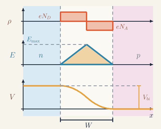
A p–n junction is one crystal doped n-type on one side and p-type on the other. Diodes, LEDs, solar cells and transistors are all built from such junctions. When the two sides meet, electrons diffuse from the n side into the p side, where they are rare, and holes diffuse the other way. Each carrier that crosses and recombines leaves behind a fixed ion whose charge is no longer cancelled: a positive donor on the n side, a negative acceptor on the p side. The charge of these ions sets up a field that pushes the carriers back, and diffusion stops when the field balances it. The strip around the junction that has lost its free carriers is the depletion layer.
Figure 2. A symmetric junction, n side left and p side right. The fixed ions of the depletion layer, width W, give the charge density ρ and so the triangular field E; the shaded area under E is the drop Vbi of the potential V.Legend
x
Position across the junction, from the n side to the p side.
m
W
Width of the depletion layer.
m
ρ
Charge density of the fixed ions: positive donors on the n half of the layer, negative acceptors on the p half.
C/m3
eND
Charge density of the ionised donors: e times their number density ND.
C/m3
eNA
Size of the charge density of the ionised acceptors: e times their number density NA, equal to eND here.
C/m3
E
Electric field, pointing from the n side to the p side.
V/m
Emax
Peak of the field, at the junction.
V/m
V
Electric potential along the junction.
V
Vbi
Built-in voltage: the drop of V across the layer, equal to the shaded area under E.
V
n
The n-type region: free electrons, with positive donor ions.
p
The p-type region: holes, with negative acceptor ions.
Figure 2 follows the junction along the position x, from the n side on the left to the p side on the right, in three graphs that share the same x. The depletion layer, of width W, lies between the dashed lines.
The top graph is the charge density ρ: two blocks. The n half of the layer holds the donor ions, of charge density eND, where ND is the number of donors per unit volume. The p half holds the acceptor ions, of charge density −eNA. Here the doping is the same on both sides, NA=ND, as in the silicon example below, so the two halves are equal, each W/2 wide. Outside the layer the free carriers cancel the ions, and ρ=0.
The middle graph is the field E. Gauss's law in one dimension, dE/dx=ρ/ε with ε the permittivity of the crystal, says that the slope of the field is the charge density divided by ε. A constant ρ therefore gives a straight line. E is zero outside the layer, rises steadily across the positive half, peaks at Emax at the junction and falls back to zero across the negative half. The result is a triangle, and the field points from n to p all the way across, as it must to push electrons back to the n side and holes back to the p side.
The bottom graph is the potential V. The potential is minus the integral of the field, dV/dx=−E, so V is flat wherever E=0 and falls across the layer by the area under the field triangle, 21EmaxW. That area is shaded in the middle graph, and the drop it produces is bracketed at the right of the bottom graph: it is the built-in voltage Vbi.
The size of Vbi follows from equilibrium. To reach the p side, an electron on the n side must climb a potential-energy step eVbi. In equilibrium the electrons obey the Boltzmann factor across that step, so their density on the p side equals their density on the n side times e−eVbi/kBT. On the n side the density is ND; on the p side, by the law of mass action, it is ni2/NA. Setting ni2/NA=NDe−eVbi/kBT and taking logarithms,
Vbi=ekBTln(ni2NAND)
For silicon with NA=ND=1016cm−3 and kBT/e=0.02585V, this is 0.02585⋅ln(1012)≈0.71V. Since ni2 carries the factor e−Eg/kBT, eVbi equals Eg minus a term that shrinks only slowly as the doping rises, so the step approaches Eg/e but cannot much exceed it. The heavily doped LED of the animation comes close, with Vbi=1.8V against Eg/e=1.9V.
The width of the layer follows from the same three graphs. With equal doping N on both sides, each half has width W/2. Across that distance the field rises with slope eN/ε, so its peak is Emax=eN(W/2)/ε. The voltage across the layer is the area of the triangle:
21EmaxW=4εeNW2
At zero bias this voltage is Vbi. A forward bias V, which makes the p side more positive, opposes the built-in field and leaves Vbi−V across the layer; a reverse bias is a negative V. The voltage across the layer is proportional to W2, so
W∝Vbi−V
For the silicon junction above, with ε≈1.0×10⁻¹⁰F/m, the layer is W≈0.43μm wide at zero bias, and the peak field Emax is near 3×10⁶V/m. A reverse bias of 5 V widens it to 1.2μm. In the animation the forward bias lowers the barrier from 1.8 eV to 0.1 eV, so the layer shrinks to 0.1/1.8≈0.24 of its width.
A junction with a built-in voltage looks like a battery, yet a wire joining its two ends carries no current. The wire makes two new contacts, metal to n and metal to p, each with its own potential step, and at a single temperature the steps around the loop add up to zero. If they did not, the loop would turn heat from surroundings at one temperature into work for ever, which the second law of thermodynamics forbids. Like a ratchet and pawl in a gas at one temperature, a junction cannot rectify its own thermal noise. Heat one contact and the balance breaks: that is the thermoelectric effect used in a thermocouple.
Rectification: two streams out of balance
A diode passes current easily in one direction and hardly at all in the other. To see why, follow the holes that cross the junction in each direction; the electrons behave in the same way and add to the same current.
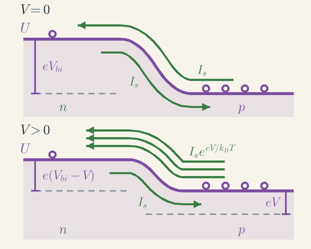
Figure 3. Potential energy U of a hole (rings) across the junction. Top: at V=0 the stream of holes climbing the step eVbi equals the stream sliding down it, Is. Bottom: a forward bias V lowers the step and multiplies only the climbing stream. Not to scale.Legend
U
Potential energy of a hole at each position across the junction.
J
n
The n side, where holes are rare (minority carriers).
p
The p side, where holes are plentiful (majority carriers).
V
Forward bias: the applied voltage, positive on the p side.
V
eVbi
Height of the step for holes at zero bias: e times the built-in voltage.
J
eV
How far the forward bias raises the level of the p side.
J
e(Vbi−V)
Height of the step under forward bias.
J
Is
Saturation current: the stream of minority holes sliding down the step; at zero bias the climbing stream equals it.
A
IseeV/kBT
The climbing stream under forward bias: eeV/kBT times larger than Is.
A
Figure 3 draws the potential energy U of a hole at each point across the junction, n side on the left and p side on the right; the rings are holes. The field of the depletion layer pushes holes towards the p side, so a hole has more potential energy on the n side: higher by eVbi when no voltage is applied (top panel). A hole going from p to n must climb this step; one going from n to p slides down it.
Two streams of holes therefore cross the junction. The first climbs. Holes are plentiful on the p side, where they are the majority carriers, but only the few with thermal energy above the step get over it. The second slides down. Holes are rare on the n side, where they are minority carriers made thermally, but any that wander into the layer are swept down the step by its field. This downhill stream depends only on how many minority holes reach the layer, not on how high the step is; it is the saturation current Is. At V=0 there is no net current, so the climbing stream must equal it, and the top panel shows one arrow labelled Is each way.
In the bottom panel a forward bias V raises the p side by eV; the dashed line beneath it marks its old level. The step falls to e(Vbi−V), and the layer narrows to match. The number of holes energetic enough to climb grows by the Boltzmann factor eeV/kBT, so the climbing stream becomes IseeV/kBT, while the downhill stream is still Is. The figure draws the larger stream as three arrows instead of one; the true factor is vastly larger, about 6×10¹¹ at 0.7 V in silicon, which is why the figure is not to scale.
In symbols, the climbing stream is proportional to ppe−e(Vbi−V)/kBT, where pp is the density of holes on the p side. A forward bias multiplies it by eeV/kBT, while the downhill stream keeps its value Is. The net hole current is the difference, IseeV/kBT−Is. The electrons give two streams of the same form, so the total current obeys the diode equation of William Shockley:
I=Is[exp(ηkBTeV)−1]
Here the ideality factor is η=1, for this picture in which carriers diffuse across the layer and recombine beyond it. A reverse bias, V<0, raises the step instead: the exponential dies away and I→−Is, only the small downhill stream. That is rectification. A forward bias of a few tenths of a volt multiplies the current many times over, while a reverse bias of any size, up to breakdown, lets through only Is.
When most carriers instead recombine inside the depletion layer, the current grows more slowly. Inside the layer np=ni2eeV/kBT, and recombination is fastest where the two densities are equal, both about nieeV/2kBT. The current then grows only as eeV/2kBT, which means η≈2, the value used in the animation. For the animation's LED, Is is about 10−16A.
The gap, more than anything else, sets the voltage at which a diode turns on. For diffusion Is∝ni2∝e−Eg/kBT, and for recombination Is∝ni∝e−Eg/2kBT. Either way, once the current is well above Is,
I≈Ce−(Eg−eV)/ηkBT
with a prefactor C that changes only slowly with doping and temperature. The current is set by how far eV lies below Eg, so the gap, far more than the doping, decides where a diode turns on.
Reading the live current–voltage curve
The expert layer of the animation plots the LED's current I against the supply voltage V as the voltage rises. The results above explain the shape of that curve, and its numbers are a good check of them.
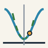
Write VT=kBT/e=25.85mV at 300 K. With η=2, ηVT=2⋅25.85=51.7mV. The current grows tenfold each time the exponent grows by ln10≈2.3, that is, every 2.3⋅51.7≈119mV. So the curve hugs the axis up to about 1.5 V (0.37 mA), bends sharply between 1.6 and 1.8 V, and reaches 20 mA at 2.0 V. The dashed gold line marks Eg/e=1.9V.
Why does the junction work about 0.2 V below Eg/e? For this LED C≈0.96A. A current of 20 mA lies log10(0.96/0.020)≈1.7 decades below C, so by the formula above the junction voltage Vj sits 1.7⋅119≈200mV below Eg/e, at 1.70 V. A silicon diode, with η≈1, has C about eight decades above its working current, so its knee falls near 0.6–0.7 V, about half a volt under its 1.12 V gap.
The supply must also push the current through the chip's series resistance of 15 Ω. At 20 mA that takes 0.020⋅15=0.30V, the rest of the 2.0 V. This resistance shapes the top of the curve. The junction's own dynamic resistance, dVj/dI=ηVT/I, is only about 2.6Ω at 20 mA, much less than 15 Ω, so the curve straightens into a line of slope about 1/(17.6Ω). On the band diagram the barrier label follows e(Vbi−Vj), which falls from 1.8 eV to 0.10 eV as the voltage rises.
Worked problem: the LED as a solar cell
Run the junction backwards: instead of putting a current in to get light out, shine light in and take power out. The same equations then describe a solar cell, and the animation's LED shows how much power one junction can deliver and why its voltage stays below Eg/e.
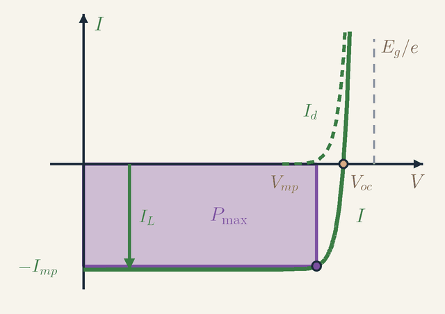
Figure 4. The animation's junction in light: the dark curve Id (dashed) moves down by the photocurrent IL to give I, which is zero at Voc. The largest rectangle under the axis with a corner on the curve has area Pmax. Drawn from the animation's model.Legend
V
Voltage across the junction, positive in the forward direction.
V
I
Current through the lit junction, I=Id−IL.
A
Id
Current of the junction in the dark: the diode equation.
A
IL
Photocurrent: the current the light drives backwards through the junction, which shifts the curve down.
A
Voc
Open-circuit voltage: where the lit curve crosses I=0.
V
Vmp
Voltage at the maximum-power point, the corner of the largest rectangle.
V
Imp
Current delivered at the maximum-power point; the lit curve is at −Imp there.
A
Pmax
Greatest power the cell delivers: the area of the shaded rectangle.
W
Eg/e
The band gap divided by e: the voltage that Voc approaches but stays below.
V
Figure 4 plots the current I through the junction against the voltage V across it, both positive in the forward direction. The dashed curve Id is the junction in the dark, given by the diode equation, with its knee just below Eg/e, the dashed vertical line.
Now light falls on the junction and creates electron–hole pairs at a rate equivalent to IL=20mA, that is, IL/e pairs per second. The field of the depletion layer sweeps each pair apart, the electron to the n side and the hole to the p side. That is a current through the junction in the reverse direction, and its size does not depend on V. The lit curve I is therefore the dark curve moved down by IL, as the arrow labelled IL shows.
The lit curve cuts the I axis at −IL and the V axis at the open-circuit voltage Voc. Between these two points V is positive and I negative: the current leaves by the positive terminal, as from a battery, so the junction delivers power. At any point of that stretch the power is the area of the rectangle between the axes and the point on the curve. The shaded rectangle, with its corner at Vmp and −Imp, is the largest, and its area is Pmax.
In equations, the lit current is
I=Is[exp(ηkBTeV)−1]−IL
With the terminals shorted, V=0 and I=−IL=−20mA: the whole photocurrent flows round the wire, backwards through the diode. With the terminals open, I=0, so the diode current must equal IL, which gives
Voc=ηVTln(1+IsIL)=1.70V
This is exactly the junction voltage at 20 mA in the animation, because in both cases the diode current is 20 mA.
The power delivered is P=V(IL−Id), where Id is the dark current at the voltage V. It is zero at both ends of the stretch and largest in between, where dP/dV=0: the corner of the largest rectangle in Figure 4. Solving numerically gives Vmp≈1.52V and Imp=IL−Id≈19.3mA, so Pmax≈29.5mW. The fill factor compares this rectangle with the box of area VocIL around the curve: 29.5/(1.70⋅20)≈0.87.
Each pair absorbed at least 1.9 eV but delivers only 1.52 eV: the voltage stays below Eg/e by the same logarithm that put the knee below it. With the 15 Ω series resistance included, the best output falls to about 24 mW. Real solar cells use gaps near 1.1–1.4 eV, a compromise: a smaller gap absorbs more of sunlight, a larger one delivers more energy per electron.
Limits of validity
The diode equation assumes low injection: far fewer injected carriers than majority ones. So the junction voltage must stay well below Vbi; the animation's 1.70 V against 1.8 V is at the edge, where the series resistance already dominates. It assumes Boltzmann statistics, which fail above roughly 1019cm−3 of doping in silicon. It treats the densities as smooth averages, yet a region 10 nm across doped at 1018cm−3 holds a single dopant atom on average.
In reverse, I=−Is holds only up to breakdown. In heavily doped junctions the barrier is so thin that electrons tunnel through it at a few volts (Zener breakdown); in lightly doped ones, carriers accelerated by the field knock out new pairs in an avalanche at tens or hundreds of volts.
Light emission has its own limit. In silicon the bottom of the conduction band and the top of the valence band lie at different crystal momenta ℏk, which differ by about 1.0×10⁻²⁴kg⋅m/s: some 1700 times the momentum of a 1.12 eV photon. The photon cannot carry the difference, so each recombination must also create or absorb a phonon, a quantum of lattice vibration. That takes up to milliseconds, other processes win, and the energy ends as heat. In direct-gap materials, such as GaAs, AlGaInP for red and InGaN for blue, both band edges lie at the same k, and electrons and holes recombine by emitting light within nanoseconds.
Where this leads
Two junctions back to back, n–p–n, make a bipolar transistor: a small current into the thin middle layer controls a much larger one through it. In a field-effect transistor a gate voltage opens or closes a conducting channel instead. With light in and power out, a junction is the solar cell of the worked problem; with mirrors and strong injection, stimulated emission turns it into a laser. Zener and tunnel diodes rely on tunnelling through a thin depletion layer, the subject of Schrödinger's Equation and Tunnelling, and the bands come from electron waves interfering on a lattice, as in Wave–Particle Duality. The Boltzmann factors are those of Kinetic Theory of Gases, and the junction that drives no current is The Second Law of Thermodynamics and Entropy at work.
Key formulas
Photon energy from recombination
hf≈Eg
When a conduction electron falls into a hole, the pair disappears and its energy leaves as a single photon. Electrons and holes gather within about kBT of their band edges, so the photon energy is close to the gap. It is the rule for an atom emitting light as an electron falls between two levels, with the two bands in place of the levels.
Symbols
h
Planck constant, 6.626×10⁻³⁴J⋅s
J⋅s
f
frequency of the emitted photon
Hz
Eg
band gap (1eV=1.602×10⁻¹⁹J)
J
When it holds: Holds for band-to-band recombination in a direct-gap material. In an indirect-gap material such as silicon a lattice vibration shares the energy and momentum, and most recombination gives heat instead of light; light from impurity levels has less energy than the gap.
Example: The LED of the animation: Eg=1.9eV=3.04×10⁻¹⁹J, so f=Eg/h≈4.6×1014Hz.
Wavelength from the band gap
λ=Eghc≈Eg1240eV⋅nm
Light of frequency f has wavelength λ=c/f, so hf≈Eg gives λ=hc/Eg. Because hc≈1240eV⋅nm, dividing 1240 by the gap in electronvolts gives the wavelength in nanometres. The wider the gap, the shorter the wavelength: infrared, red, green, then blue.
Symbols
λ
vacuum wavelength of the emitted light (in nm with the 1240 form)
m
h
Planck constant
J⋅s
c
speed of light, 3.00×10⁸m/s
m/s
Eg
band gap (in eV with the 1240 form)
J
When it holds: Same conditions as hf≈Eg. The real emission line is some 20 nm wide, because the carriers are spread over about kBT above the band edges.
Example:Eg=1.9eV: λ≈1240/1.9≈653nm, red; GaAs, 1.42 eV: about 873 nm, infrared.
Law of mass action for electrons and holes
np=ni2,ni∝exp(−2kBTEg)
Pairs are created thermally at a rate proportional to e−Eg/kBT and destroyed when electrons meet holes, at a rate proportional to np. Equal rates in equilibrium make np a constant of the material at a given temperature, whatever the doping. In a pure crystal n=p=ni, so ni carries half the exponent.
Symbols
n
density of conduction electrons
m−3
p
density of holes
m−3
ni
intrinsic density, that of the pure crystal
m−3
Eg
band gap
J
kB
Boltzmann constant, 1.381×10⁻²³J/K
J/K
T
absolute temperature
K
When it holds: Thermal equilibrium (no bias, no light) and doping below about 1019cm−3 in silicon. Under forward bias or light np exceeds ni2 (under reverse bias it falls below), and that excess is what drives a diode or a solar cell. The full ni also carries a slower factor T3/2.
Example: Silicon at 300 K with 1016 donors per cubic centimetre: p=(1010)2/1016=104cm−3.
Diode equation
I=Is[exp(ηkBTeV)−1]
Two flows of carriers cross the junction: majority carriers climbing the barrier, a flow proportional to eeV/kBT, and minority carriers swept down it by the field, a flow independent of V. The current is their difference, and the two cancel at V=0. Forward bias (V>0) makes the current grow exponentially; reverse bias leaves only the leak −Is.
Symbols
I
current through the diode, positive from p to n
A
Is
saturation current
A
e
elementary charge, 1.602×10⁻¹⁹C
C
V
voltage across the junction, positive for forward bias
V
η
ideality factor, between 1 and 2
kB
Boltzmann constant
J/K
T
absolute temperature
K
When it holds: Low injection (junction voltage well below Vbi) and reverse voltages below breakdown. At high current the drop across the chip's series resistance must be added: 0.30 V at 20 mA across 15 Ω in the animation.
Example: The LED of the animation: Is≈1.05×10⁻¹⁶A and η=2; at V=1.70V across the junction, I=20mA.
Thermal voltage
VT=ekBT≈25.9mV(300K)
The voltage through which a charge e must move to gain the typical thermal energy kBT. It is the natural voltage scale of every junction: the diode current changes by a factor of e≈2.718 for each ηVT of bias. It grows in proportion to the absolute temperature.
Symbols
VT
thermal voltage
V
kB
Boltzmann constant
J/K
T
absolute temperature
K
e
elementary charge
C
When it holds: The definition holds at any temperature; the value 25.9 mV is for 300 K (25.7 mV at 25 °C).
Example:1.381×10−23⋅300/(1.602×10−19)≈0.0259V; with η=2 the diode of the animation has ηVT=51.7mV.
Voltage step for a given current ratio
ΔV=ηVTln(I1I2)
Far above Is the −1 in the diode equation can be dropped, so the current is a pure exponential of the voltage. Dividing two currents cancels Is, and the logarithm gives the voltage difference. Every factor of ten in current costs the same 2.3ηVT, which is why the curve looks like a sharp knee on a linear scale.
Symbols
ΔV
increase of the junction voltage
V
η
ideality factor
VT
thermal voltage
V
I2
final current
A
I1
initial current
A
When it holds: Both currents well above the saturation current, small enough for the drop across the series resistance to be negligible, and at the same temperature.
Example: In the LED of the animation (η=2), going from 2 mA to 20 mA raises the junction voltage by 2⋅25.85⋅ln10≈119mV.
Width of the depletion layer
W∝Vbi−V
The depletion layer holds fixed ions of uniform density. By Gauss's law the field inside grows linearly with depth and the potential quadratically, so the voltage across the layer grows as W2. Forward bias (V>0) leaves less voltage across the layer and narrows it; reverse bias (V<0) widens it.
Symbols
W
thickness of the depletion layer
m
Vbi
built-in voltage
V
V
applied voltage across the junction, positive for forward bias
V
When it holds: An abrupt junction with uniform doping on each side (a gradual one gives a cube root instead), with V below Vbi.
Example: Silicon with 1016 dopants per cubic centimetre on both sides: 0.43 µm at zero bias, 0.43⋅5.71/0.71≈1.2μm at 5 V reverse.
Series resistor for an LED
R=IVs−VF
The resistor and the LED carry the same current and share the supply voltage. The LED takes roughly its forward voltage VF at its working current, so the resistor takes the rest, and Ohm's law gives its value. Because the current through a resistor varies only linearly with its voltage, it holds the current steady where the LED's steep curve could not.
Symbols
R
resistance in series with the LED
Ω
Vs
supply voltage
V
VF
forward voltage of the LED at the chosen current
V
I
chosen current
A
When it holds: The supply must be comfortably above VF: if the two are close, a small change of VF (with temperature, or from one LED to the next) changes the current a lot. The resistor must also handle the power (Vs−VF)I.
Example: Blue LED, VF=3.0V, 20 mA from 5.0 V: R=2.0/0.020=100Ω.
Glossary
Semiconductor
A solid whose band gap is small enough, a few electronvolts at most, for heat or light to lift some electrons across it. Its conductivity lies between that of metals and insulators, and doping, light and temperature change it enormously.
Valence and conduction bands
The valence band holds the bonding electrons and is full in a pure crystal at low temperature; the conduction band above it is almost empty, and electrons in it move freely. A completely full band carries no current, so conduction needs electrons in the upper band or holes in the lower one.
Hole
An empty state in an almost full valence band. Neighbouring electrons move into it, so the hole moves like a particle with charge +e and a positive mass; it is a missing electron, not a missing atom.
Effective mass
The mass m∗ with which an electron or hole near a band edge responds to forces, as if it were free: E≈ℏ2k2/2m∗. It depends on how easily electrons hop between atoms, from about 0.07me for electrons in GaAs to about me.
Doping
Adding a tiny, controlled amount of impurity, often one atom per million or fewer. Donors such as phosphorus give free electrons (n-type material), acceptors such as boron give holes (p-type); the crystal stays neutral, because each free carrier is balanced by a fixed ion.
Majority and minority carriers
In doped material, the carriers supplied by the dopant are the majority and the other kind the minority, with np=ni2. Silicon with 1016 donors per cubic centimetre has 1016 electrons but only 104 holes per cubic centimetre.
p–n junction
The boundary between p-type and n-type regions of one crystal. It conducts easily in one direction and hardly at all in the other, so it is a diode; lit instead of driven, it is a solar cell or photodiode.
Depletion layer
The thin region at a junction emptied of free carriers, where only the fixed donor and acceptor ions remain. Their charge creates the electric field and the built-in voltage; the layer narrows under forward bias and widens under reverse bias.
Forward and reverse bias
Forward bias connects the p side to the + terminal and lowers the barrier, so the current grows exponentially with the voltage. Reverse bias raises the barrier, and only the tiny saturation current flows until breakdown.
Recombination
A conduction electron falling into a hole, which destroys the pair. The energy, about Eg, leaves as a photon in an LED, or as lattice vibrations (heat) in silicon and at defects.
Light-emitting diode (LED)
A p–n junction in a direct-gap material, driven in forward bias so that electrons and holes recombine in it and emit light of wavelength λ≈hc/Eg. The material sets the colour; the current sets the brightness. It is driven through a series resistor R=(Vs−VF)/I, in ohms, where Vs is the supply voltage and VF the LED's forward voltage at the working current I.
Direct and indirect band gap
In a direct gap (GaAs, InGaN) the two band edges lie at the same crystal momentum, so an electron can drop by emitting a photon alone. In an indirect gap (silicon) a lattice vibration must also take part, so light emission is very weak.
Quantities
Eg
Band gap
J
The energy from the top of the valence band to the bottom of the conduction band, usually quoted in electronvolts (1eV=1.602×10⁻¹⁹J): 1.12 eV for silicon, 1.9 eV for the LED of the animation.
λ
Wavelength of the emitted light
m
Set by the gap, λ≈hc/Eg, and usually quoted in nanometres: 653 nm (red) for 1.9 eV, 460 nm (blue) for 2.7 eV. Here h=6.626×10⁻³⁴J⋅s is the Planck constant, c=3.00×10⁸m/s the speed of light and f=c/λ the photon frequency in hertz.
n
Electron density
m−3
The number of conduction electrons per unit volume. Semiconductor densities are usually quoted per cubic centimetre: 1cm−3=106m−3.
p
Hole density
m−3
The number of holes per unit volume; in n-type material it is pushed down to ni2/n.
ni
Intrinsic carrier density
m−3
The electron and hole density of the pure crystal, about 1010cm−3 in silicon at 300 K. It rises steeply with temperature and falls steeply as the gap widens.
Is
Saturation current
A
The reverse current that a diode cannot block, carried by minority carriers swept across the junction; it also sets the scale of the forward current. About 10−16A for the LED of the animation. The diode current I (in amperes, positive from p to n) at junction voltage V (in volts, positive for forward bias) is I=Is[exp(eV/ηkBT)−1]. Far above Is, raising V by ΔV takes the current from I1 to I2, with ΔV=ηVTln(I2/I1).
η
Ideality factor
1 when carriers cross the junction by diffusion, close to 2 when they recombine inside the depletion layer; the current grows tenfold for every 2.3ηVT.
VT
Thermal voltage
V
kBT/e, with kB=1.381×10⁻²³J/K the Boltzmann constant, T the absolute temperature in kelvin and e=1.602×10⁻¹⁹C the elementary charge: the voltage that gives a charge e the typical thermal energy kBT, 25.9 mV at 300 K.
Vbi
Built-in voltage
V
The potential step across an unbiased junction: about 0.7 V in silicon, 1.8 V in the LED of the animation. A voltmeter cannot measure it, because its own contacts add steps that cancel it.
W
Depletion width
m
The thickness of the depletion layer, typically 0.1–1 µm; it varies as Vbi−V, narrowing under forward bias.
Quiz
Beginner What is a “hole” in a semiconductor?
A gap in the crystal where a whole atom is missing
A proton that has broken free from its atom
A place where an electron is missing, which moves like a positive charge
A part of the chip where current can never flow
Show answer
Answer: C. A place where an electron is missing, which moves like a positive charge
When an electron leaves a bond, a neighbouring electron can jump into the empty place, so the empty place moves. It lacks one electron's negative charge, so it behaves like a positive charge.
Beginner A battery is connected to an LED the wrong way round. What happens?
Almost no current flows and the LED stays dark
The LED lights up with a different colour
The LED lights up just as before
The LED glows at half its usual brightness
Show answer
Answer: A. Almost no current flows and the LED stays dark
An LED is a diode: its p–n junction lets current through in one direction only. Reversed, the barrier at the junction gets higher, almost no current flows and there is no light.
Beginner What mainly decides the colour of the light from an LED?
How much current flows through it
The colour of its plastic cap
How long it has been switched on
The semiconductor it is made from
Show answer
Answer: D. The semiconductor it is made from
Each electron that drops into a hole gives up an energy set by the material (its band gap), and that energy fixes the colour. More current gives more light of the same colour; a tinted cap only filters it.
Intermediate An LED is made from a semiconductor with a band gap of 2.3 eV. Roughly what wavelength does it emit? (h·c ≈ 1240 eV·nm)
≈ 650 nm (red)
≈ 540 nm (green)
≈ 2850 nm (infrared)
≈ 430 nm (violet)
Show answer
Answer: B. ≈ 540 nm (green)
λ = h·c / E_g ≈ 1240 eV·nm ÷ 2.3 eV ≈ 540 nm, green light. Multiplying instead of dividing gives the 2850 nm distractor.
Intermediate Is a piece of n-type silicon negatively charged?
Yes, because it contains extra electrons
Yes, but only while a current flows
No: each spare electron is balanced by a fixed positive donor ion
No: the spare electrons leave the crystal straight away
Show answer
Answer: C. No: each spare electron is balanced by a fixed positive donor ion
Each phosphorus atom is neutral when it enters the crystal. Its fifth electron becomes free and the atom stays behind as a fixed positive ion, so the material as a whole remains neutral.
Intermediate Why does the resistance of a pure (undoped) semiconductor fall when it is heated, while that of a metal rises?
Heat lifts more electrons across the band gap, creating more electron–hole pairs
The atoms vibrate less, so the electrons collide less often
Heating drives the impurities out of the crystal
The band gap gets much wider, so the electrons move faster
Show answer
Answer: A. Heat lifts more electrons across the band gap, creating more electron–hole pairs
The number of free carriers grows rapidly with temperature because more electrons get enough thermal energy to cross the gap. This outweighs the extra collisions, which dominate in metals. (The gap actually narrows slightly on heating.)
Advanced A silicon diode (ideality factor η = 1) at 300 K carries 1 mA. Roughly how much must the forward voltage increase for it to carry 10 mA?
About 0.6 V
About 26 mV
About 0.9 V
About 60 mV
Show answer
Answer: D. About 60 mV
Well above I_s, I ∝ exp(e·V / η·k_B·T), so a tenfold increase needs ΔV = η·V_T·ln 10 ≈ 25.9 mV × 2.30 ≈ 60 mV. 26 mV is V_T itself, and 0.6 V is a typical total forward voltage, not the change.
Advanced Silicon is the most common solar-cell material, yet it makes very poor LEDs. Why?
Its band gap is too small for it to emit any photon
Its band gap is indirect, so recombination also needs a phonon and mostly produces heat
Silicon cannot be doped p-type
Its electrons and holes never meet at a junction
Show answer
Answer: B. Its band gap is indirect, so recombination also needs a phonon and mostly produces heat
In silicon the lowest conduction-band states and the highest valence-band states have different crystal momenta. A photon carries almost no momentum, so radiative recombination also needs a phonon and is very slow; non-radiative processes win. LEDs use direct-gap compounds such as GaAs, AlGaInP or InGaN.
 Physics Tutor